En länk till val av lösenord har skickats till: För att komma åt dina inköp behöver du ett lösenord.
Få 3 videor eller 25 bilder med en kostnadsfri provperiod
Nya filter har lagts till
Sortera efter

33 263 resultat för kisel i videor

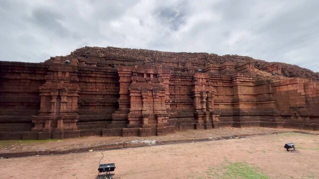
Si Thep Historical Park, Phetchabun, Thailand. An architecture in the Dvaravati period. Si Thep Historical Park is new world heritage site in Phetchabun Province, Thailand
00:13
HD
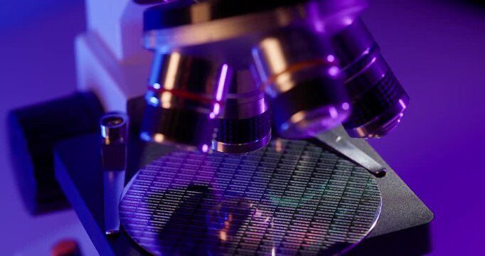
silicon wafer for manufacturing semiconductor of integrated circuit.Electronic circuit designs have been built onto the wafers using micromaching including photolithography
00:30
HD
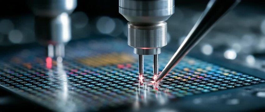
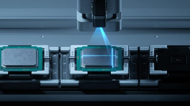
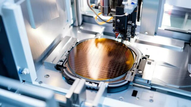
Advanced semiconductor manufacturing equipment processing silicon wafer with laser
00:10
HD
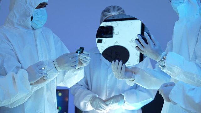
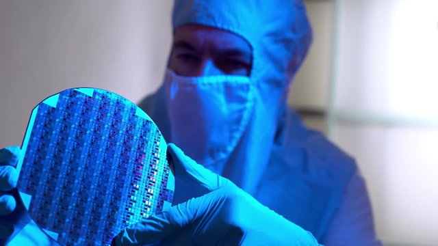
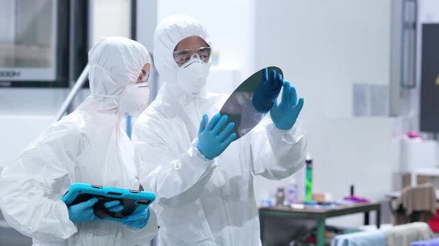
Team of scientist wearing protective hazmat suit safety goggle hairnet surgical mask inspect silicon wafer round disk inside semiconductor research laboratory cleanroom
00:07
HD
High speed processor chip animation video with neon circuit connections, advanced semiconductor computing technology, powerful ai data processing and modern electronics background
00:08
HD
Cleanroom team discusses a silicon wafer and tablet data together during a collaborative semiconductor microchip quality inspection in a sterile hitech manufacturing facility
00:11
HD
Glowing HBM memory stack chip on circuit board AI data center hardware
00:08
HD
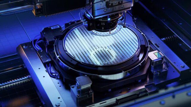
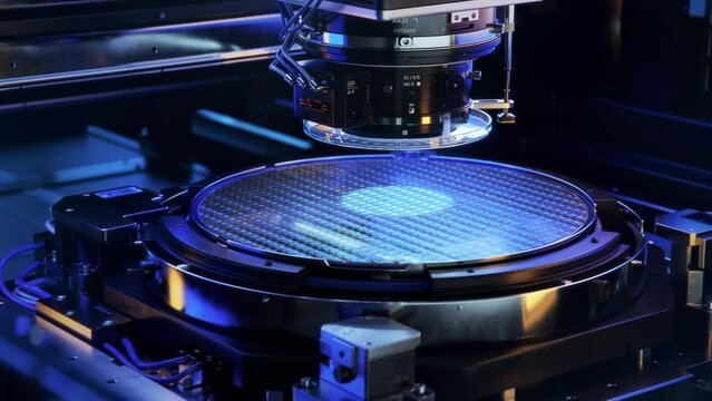
Silicon Wafer during Photolithography Process. Shot of Lithography Process that allows to Create Complex Patterns on a Wafer during Semiconductor and Computer Chip Manufacturing at Modern Foundry.
00:11
HD
Large stone Thammachak in Si Thep Historical Park, registered as a UNESCO World Heritage Site in 2023, Phetchabun, Thailand
00:08
HD
dramatic aerial skyline of bangalore india at sunset timelapse
00:10
HD
silicon metalloid chunks
00:13
HD
Workers move monocrystalline silicon ingot on cart in solar factory
00:22
HD
Robotic arms with silicon wafers for semiconductor manufacturing 4k footage
00:08
HD
The concept of computer technology: An engineer in a sterile jumpsuit holds a computer microchip in his gloves and examines it. The concept of artificial intelligence
00:12
HD
Iridescent semiconductor wafer in seamless loop with alpha channel, futuristic microchip surface 3D render static camera overlay
00:12
HD
Particles of white dry sand are pouring down forming hill on an isolated black background. Close up shot of crumbling natural sand grains, sandy dune. Heap of petrified natural mineral.
00:41
HD
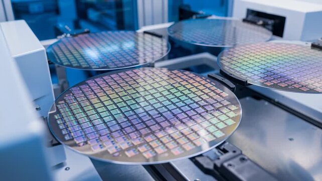
Silicon semiconductor wafer close-up. In electronics, a wafer also called a slice or substrate is a thin slice of semiconductor, a crystalline silicon, used for the fabrication of integrated circuits
00:42
HD
Aerial view of an AI supercomputing data center in Ashburn with glowing data stream animations representing large language model training and the environmental controversy of massive power consumption
00:11
HD
Silicon wafer processed in semiconductor foundry, robotic arm handling chip, clean room setting, advanced manufacturing technology, precision engineering, 4K video
00:08
HD
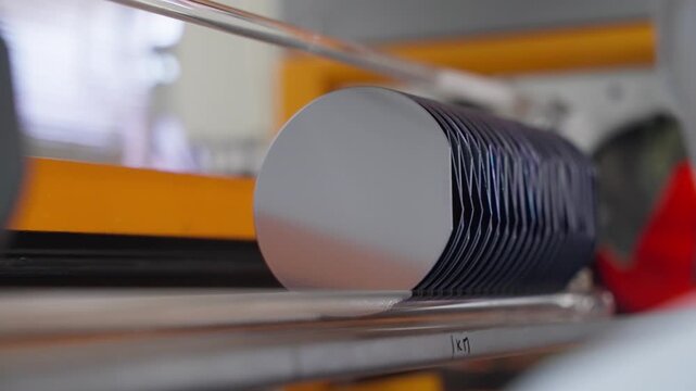
Cleanroom fabrication of silicon wafers in plastic holder boxes with integrated circuits to produce CPUs and GPUs
00:10
HD
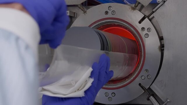
Gloved technician loading a stack of silicon wafers into a heated semiconductor processing chamber in a cleanroom, preparing for thermal treatment in advanced chip fabrication.
00:12
HD
colorful Semiconductor wafer disk made of silicon
00:20
HD
Innovative laboratory, automatic machine produces polishing of silicon wafers.
00:13
HD
silicon wafer semiconductor
00:06
HD
Green nano technology wafer production line robotics automated handling semiconductor silicon microchip circuit cleanroom manufacturing reflecting
00:05
HD
Semiconductor shortage outlook for laser circuit chip production
00:08
HD
High-tech circuit board with glowing purple light paths.
00:08
HD
Silicon Wafer during Photolithography Process. Shot of Lithography Process that allows to Create Complex Patterns on a Wafer during Semiconductor and Computer Chip Manufacturing at Fab or Foundry.
00:11
HD
Two Engineers/ Scientists/ Technicians in Sterile Cleanroom Suits Use Microscopes for Component Adjustment and Research. They Work in an Electronic Components Manufacturing Factory.
00:11
HD
Cyan electronic hex core visual circuit pathways, blue matrix, glowing processor style. tech intros, machine learning semiconductor clips, cyber security screens, digital products, motion graphics.
00:25
HD
Macro tracking shot microscope objectives adjusting over microchip silicon wafer on laboratory stage during close inspection.
00:31
HD
Futuristic modern metropolis city skyline. Capital of biggest technology innovations, startup projects, Artificial intelligence, business angels investors. San Francisco skyscrapers, Silicon valley
00:40
HD
Beautiful Clear Waterfall Cascade In Tropical Rainforest, Kuang Si Falls In Luang Prabang, Laos
00:17
HD
minimalist vertical scanning light pattern background vector svg
00:29
HD
note music animated icon symbol note music do re mi fa sol la si do green screen 4k looping
00:14
HD
Engineers Reviewing 3D Cad Design On Computer
00:23
HD
A close-up view of a silicon wafer's microprocessor circuit layout. The semiconductors or central processing unit CPU microchips are fabricated from a silicon wafer with patterned layers of materials.
00:30
HD
The Process Of Cooling Down Crystal In A Modern Photovoltaic Factory
00:23
HD
Cleanroom technicians in coveralls hold and inspect silicon wafer discs beside a microscope under controlled lighting.
00:39
HD
Kek Lok Si Temple Chinese New Year Penang Malaysia
00:11
HD
Macro dolly shot side view of a computer electrical circuit with cip, slots, microchip and microprocessors, black board with transistors and microchips. Close up detail of electronic components on PC.
00:16
HD
Silicon wafer for manufacturing semiconductor of integrated circuit.Electronic circuit designs have been built onto the wafers using micromaching including photolithography
00:31
HD
Precision Semiconductor Assembly in Automated Manufacturing
00:15
HD
Macro shot of si, er watch ticking
00:08
HD
Khao Klang Nok Si Thep Historical Park, registered as a UNESCO World Heritage Site in 2023, Phetchabun, Thailand
00:09
HD
Clean Room Process Check
00:29
HD
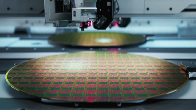
High angle macro view of silicon microchip wafer array with glowing golden green and pink light reflections during precision semiconductor manufacturing process (AI Generated)
00:05
HD
Macro Shot of Automatic Pick and Place machine quickly installs Components on Circuit Board. While board moving on assembly line. Electronics and Circuit board Manufacturing Factory.
00:09
HD
Woman Electronics Factory Worker in Blue Work Coat and Protective Glasses is Assembling Laptop's Motherboard with a Screwdriver. High Tech Factory Facility with Multiple Employees.
00:11
HD
cleanroom tech checking out a silicon wafer microchip disk 4k
00:18
HD
Aerial: Apple Campus spaceship at sunrise in Sunnyvale / Cupertino Silicon Valley, California, USA. 21 April 2022
00:24
HD
Slow motion closeup of semiconductor wafer grid sliding across production table in cleanroom with shallow depth of field tracking shot, probe view.
00:11
HD
Wide static night shot of bright golden and red fireworks exploding over the brightly illuminated Kek Lok Si Temple complex and the towering Guan Yin statue in Penang.
00:15
HD
Automated semiconductor fabrication footage of a robotic handling system transporting stacked silicon wafers through equipment inside a cleanroom microfabrication environment.
00:17
HD
Kek lok si temple aerial view circling the pagoda of ten thousand buddhas in penang
00:23
HD
Advanced semiconductor chip featuring the United States flag, symbolizing AI innovation, semiconductor manufacturing, digital technology, electronics, computing, cybersecurity
00:10
HD
A close-up view of a silicon wafer's microprocessor circuit layout. The semiconductors or central processing unit CPU microchips are fabricated from a silicon wafer with patterned layers of materials.
00:19
HD
Aerial drone top view preserve history Prasat Prang Si Thep, a World Heritage Site, is located at Si Thep, Si Thep District, Phetchabun.
00:28
HD
Aerial View of Downtown San Jose California with Highway Interchange and Silicon Valley Skyline at Sunset
00:06
HD
High-tech concept of an artificial intelligence microchip processing big data flows. 3D isometric view of glowing neural network circuits and binary code on a dark background for futuristic tech.
00:20
HD
Male and female workers in protective suits inspect silicon wafers with tablets in a semiconductor factory.
00:25
HD
Aerial View of TSMC Semiconductor Manufacturing Facility
00:12
HD
aerial view of anyang si south korea at golden light timelapse video
00:10
HD
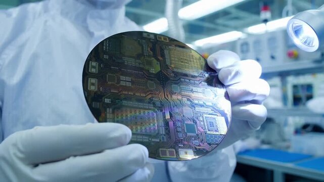
Gloved hands holding and rotating silicon wafer with iridescent microchip patterns under bright inspection lamp in cleanroom
00:10
HD
Sprawling Silicon Valley Cityscape at Sunrise
00:08
HD
Close-up of a circular silicon wafer held by metal tweezers as a liquid chemical solution is applied from a pipette, set against a bright orange background in a cleanroom laboratory setting.
00:10
HD
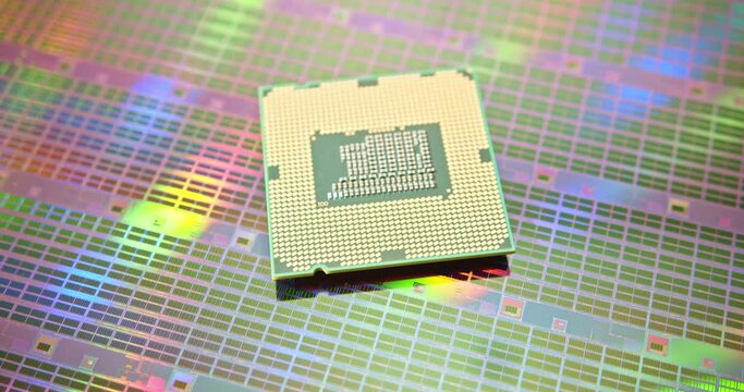
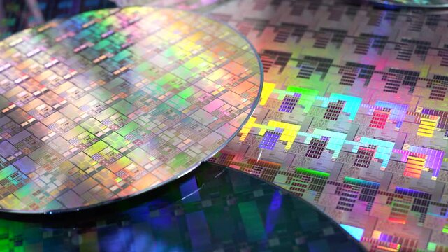
Macro of silicon wafer semiconductor with neon color, integrated circuits to manufacture CPU and GPU
00:25
HD
Semiconductor Packaging Process. Computer Chips, Silicon Die are being Extracted by a Pick and Place Machine from Semiconductor Wafer and Attached to Substrate. Computer Chip Manufacturing at Factory.
00:08
HD
Modern High-Tech Electronics Factory Moving Manufacturing Conveyor: Professionals Doing Precision Work Assemble Circuit Boards, Processors, Microchips, Semiconductors. High-Quality Production Line
00:14
HD
A silicon wafer turning on a stage, die grid visible
00:10
HD
Futuristic rotating hud circle with glowing silicon intelligence Si logo for super AI network concept
00:06
HD
Atomic force microscopy infographic animation showing a nanoscale surface scan with a silicon probe, optical lever beam, and a quadrant photodetector mapping an atomic crystal terrace in 3D
00:59
HD
Explore the intricate process of semiconductor manufacturing as machinery works on silicon wafers. This high-tech facility operates efficiently to create cutting-edge technology
00:10
HD
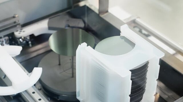
Automated semiconductor wafer handling system lifting a silicon substrate from a protective cassette inside cleanroom equipment, precision robotics in microelectronics manufacturing
00:05
HD
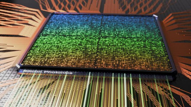
Abstract 3d render of a silicon chip with photonic interconnect. Silicon Photonic is labeled on the interface.
00:10
HD
Hoover Tower with red dome rising above red tile campus buildings, lush tree canopy and Silicon Valley sprawl stretching toward distant mountains under cloudy sky. California. Aerial view. Quiet scene
00:10
HD
Back view of female tourists walking into ancient architecture at Si Thep historical park new world heritage site in Phetchabun, Thailand. New UNESCO archaeological site in Petchabun Thailand
00:14
HD
Dynamic microchip circuitry with flowing lights and technology pulse
00:10
HD
technician with wafer
00:22
HD
Close-up of an engineer soldering a circuit board on an electronic microchip
00:10
HD
A male worker in protective clothing inspects silicon wafers at a semiconductor factory.
00:28
HD
Aerial drone top view preserve history Prasat Prang Si Thep, a World Heritage Site, is located at Si Thep, Si Thep District, Phetchabun.
00:16
HD
A close-up view of advanced semiconductor wafer processing inside a modern cleanroom facility, showcasing precision machinery, high-tech innovation, and futuristic chip manufacturing technology
00:05
HD
Careful researcher carrying silicon wafer in microchip manufacturing facility, trialing advanced materials. Expert wearing bunny suit inspecting delicate semiconductor substrates, camera B
00:22
HD
Factory Clean Room Laboratory. Industrial Engineer
00:14
HD
Semiconductor wafer animation loop, colorful silicon wafers with microchip patterns, futuristic technology background, 3D render
00:12
HD
Blue microchip circuit background glowing processor core, connected electronic traces, deep digital depth. hardware semiconductor promos, AI technology intros, computing explainers, futuristic circuit
00:20
HD
Wide Shot Inside Bright Advanced Semiconductor Production Fab Cleanroom with Working Overhead Wafer Transfer System
00:08
HD
Semiconductor Production At Electronics Manufacturing Facility: Two Specialists In Sterile Suits Taking Out Silicon Wafer From Soldering Jet Printer And Checking It. Engineers Making Computer Hardware
00:15
HD
Aerial drone top view preserve history Prasat Prang Si Thep, a World Heritage Site, is located at Si Thep, Si Thep District, Phetchabun.
00:24
HD
Polydimethylsiloxane, rotating 3D model of silicone polymer, seamless looped video, molecular structure with selective focus
00:15
HD
Computer CPU chip on silicon wafer. close up shot of electronic system with data processing.  Chip, AI calculating big data abstract. 3D rendering, 4K loop
00:08
HD
sunny day bangalore cityscape downtown aerial panorama tlmelapse 4k india
00:05
HD
Macro shot of a computer CPU processor on a heatsink with copper heatpipes and blue ambient light
00:07
HD
A close-up view of a silicon wafer's microprocessor circuit layout. The semiconductors or central processing unit CPU microchips are fabricated from a silicon wafer with patterned layers of materials.
00:19
HD
Aerial,Birdseye view towards Wat Si Chum Buddha Statue at Sukhothai,footage stops on the top of the Buddha Statue at its top.
00:25
HD
Travel concept. Ancient sites, tourist attractions in Sukhothai, Thailand. Rear view of tourist woman walking into Wat Si Chum temple in Sukhothai, Thailand. UNESCO site or World heritage site
00:22
HD
Holofiber synthetic pillow filler close-up.
00:27
HD
Technician holding an electric circuit layout. Photomask for printed circuit boards
00:05
HD
automatic robot arm with silicon wafers and microcircuits and Automation system control application in smart factory
00:30
HD